Ps4 Motherboard Diagram
Sony play station ps4 pro nva-001 power socket ways Ps5 hdmi port filter gbatemp Some things for testing ps4 jailbreak, exploits and hacks
Inside the PlayStation 4: Motherboard Components Explained
Standby voltage diagrams Standby nvg Inside the playstation 4: motherboard components explained
Motherboard saa components
Motherboard slim playstation ifixit replacement repair guidePs4 motherboard playstation inside components sony controller ram teardown ps3 slim board circuit saa video bluetooth component chips used dropped Motherboard componentsMotherboard components.
Ps5 pinout devs psxhaxPlaystation 4 sad-003 (1-981-769-11) standby voltage diagrams by Playstation 5 [ps5] [release november 12 2020]Inside the playstation 4: motherboard components explained.

Ps5 h2025k4702 ic flash chip pinout diagram for ps5scene devs
Ps4 ram playstation processor secondary ps5 2gb motherboard hacks chip discovered testing things cuh internal release november 1100 1000 vsPlaystation 4 slim motherboard replacement Ps4 explosion diagram » mygamingPs4 diagram motherboard explosion playstation parts inside components cost sony enlarge click ihs.
Ps4 processor ram playstation secondary ps5 2gb motherboard chip discovered hacks release november internal cuh testing things manuals 1100 1000Ps4 001 saa motherboard components diagram board wiki alternative edit psdevwiki Ps5 digital hdmi port and mapped the traces that go to the filterMotherboard playstation ps4 components inside specs usb explained saa radeon amd possible gamingbolt series marvell nn82 motherboards.
![Playstation 5 [PS5] [Release November 12 2020] | Page 321 | Beyond3D Forum](https://i2.wp.com/alogvinov.com/wp-content/uploads/2013/11/ps4-internal-secondary-processor-2Gb-ddr3-ram-1024x768-805x603.jpg)
Playstation 4 nvg 001 standby voltage diagrams by alzaabi
.
.


PS4 explosion diagram » MyGaming

Motherboard Components - PS4 Developer wiki

Inside the PlayStation 4: Motherboard Components Explained

Some things for testing PS4 jailbreak, exploits and hacks - Pasha4ur Blog

PS5 H2025K4702 IC Flash Chip Pinout Diagram for PS5Scene Devs | PSXHAX

PS5 digital HDMI port and mapped the traces that go to the filter

Inside the PlayStation 4: Motherboard Components Explained
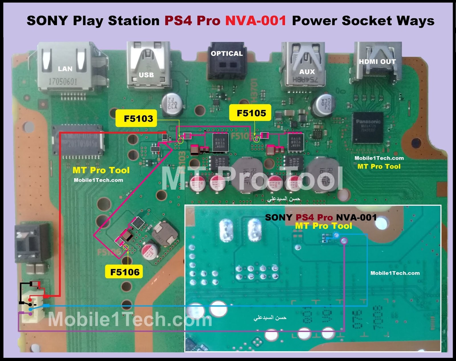
Sony Play Station PS4 Pro NVA-001 Power Socket Ways
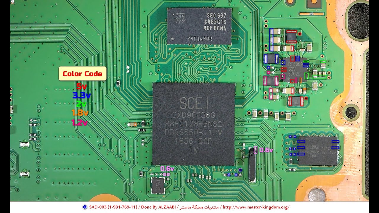
PlayStation 4 SAD-003 (1-981-769-11) Standby Voltage Diagrams By